
The trend in the electronics packaging industry is towards smaller, more powerful devices. With these small, high power components, however, there are also higher heat fluxes. As a result, engineers must find ways to minimize the thermal resistance from the electronic device junction to ambient air.
Improving Heat Transfer Between Surfaces and Overall Thermal Performance
This thermal resistance can be expressed as Rja, where:
- Rja – Thermal resistance from the device junction to ambient air or water
- Rjc – Thermal resistance from the device junction to the package case, determined by the electronic device manufacturer (designer has no direct influence)
- Rcs – Thermal resistance from the package case to the heat sink or cold plate, determined by the size and quality of the contact areas between the electronic device and the heat sink or cold plate, the materials used, and contact pressure
- Rsa – Thermal resistance from the heat sink or cold plate to ambient air or water, determined by the heat sink or cold plate design (material and geometry)
Therefore, one way to reduce Rja is to reduce Rcs, the contact resistance between the electronic device case and ambient-cooled, finned heat sinks or liquid-cooled cold plates. There are several factors that impact Rcs, including surface flatness, surface roughness, contact force or clamping pressure, surface cleanliness, and interface materials.
Surface Flatness and Surface Roughness
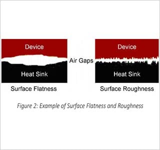
Surface flatness can be understood as widely spaced surface irregularities or “waviness” of a surface. Surface roughness is the submicron scale irregularities of a surface, usually as a result of machining, usage, and/or wear.
The contact between two imperfect surfaces will result in air gaps between them. (See Fig. 1.) Most contact areas consist of more than 90% air voids, which represent a significant resistance to heat transfer since air is not a very effective thermal conductor. Table 1 shows typical surface roughness values for different manufacturing processes.
Table 1:
| Process | Units in µm | Units in µin |
| Polishing | 0.1 – 0.4 | 4 – 16 |
| Grinding | 0.1 – 1.6 | 4 – 64 |
| Laser Cutting | 0.8 – 6.3 | 32 – 252 |
| Die Casting | 0.8 – 1.6 | 32 – 64 |
| Machining | 0.8 – 1.6 | 32 – 64 |
| Extrusion | 0.8 -3.2 | 32 – 128 |
| Drilling | 1.6 – 6.3 | 64 – 252 |
A mounting surface flatness of 0.001 in/in is generally required for satisfactory contact between the electronic device and the heat sink or cold plate. The surface roughness should be equivalent to that of the electronic device, where 32-64 µin is usually adequate. Finer finishes add unnecessary cost with little or no improvement in thermal performance. Surface flatness is typically much more critical than surface finish in achieving a good thermal interface.
Contact Force
Another very important factor in minimizing contact thermal resistance is contact force, or the force with which the electronic device is pushed against the heat sink or cold plate. Electronic device and heat sink surfaces will never be perfectly flat. Consequently, there will always be air gaps in between. However, as the contact force pushing the two surfaces together increases so does the number of contact points between the two surfaces, resulting in a lower case-to-sink thermal resistance, Rcs. This relationship between force and thermal resistance does not follow a linear curve. As contact force is increased, contact thermal resistance will decrease until a point where it will show diminishing returns in thermal resistance reduction and maximum force the package can handle is approached. The electronic device manufacturer should be contacted for recommended contact forces.
Surface Cleanliness
Mounting surface cleanliness is also important in minimizing contact thermal resistance. Mounting surfaces should be kept free of all foreign material, such as dirt, oil, oxides, and films. Since most heat sinks and cold plates are stored after machining, a cleaning operation is recommended prior to mounting the device. A satisfactory cleaning technique is to lightly polish the mounting surface with 3M Scotch Brite® No.000 fine steel wool, followed by a semiconductor cleaning solvent wipe.
Thermal Interface Material
Finally, in order to further improve Rcs, an appropriate Thermal Interface Material (TIM) should be used to fill air gaps between the two surfaces. There are a number of technologies that can be used, including thermal greases and thermally conductive compounds, elastomers, adhesive tapes, etc., each with their own characteristics (operating temperatures, ease of application, curing time, pressure requirements, etc.) that can make them more or less desirable depending on the application. Contact Boyd to consult on how to select the appropriate TIM for your application. Table 2 shows typical thermal resistance and thermal conductivity values for these TIMs.
Table 2:
| Interface | Thickness (in.) | Thermal Conductivity, k(W/m-K) | Rcs(°C/W) |
| Dry Joint | N/A | N/A | 2.9 |
| Thermal Grease | 0.003 | 0.7 | 0.9 |
| Thermal Compound | 0.005 | 1.2 | 0.8 |
| Elastomer | 0.010 | 5.0 | 1.8 |
| Adhesive Tape | 0.009 | 0.7 | 2.7 |
Thermal Interface Material
Contact conditions encompass a number of areas including surface flatness, surface roughness, surface cleanliness, contact pressure, and interface materials. There are many technologies and techniques available for optimizing the thermal path from the electronic device junction to the heat sink. It’s important to minimize the thermal resistance in order to maintain the electronic device temperature below its maximum rated value and increase the end product reliability. 


